


Printed Circuit Board design
|
Introduction: Printed circuit boards the most frequently used interconnection technology for components in electronic products. PCB requirements today have developed with the increase in the packaging density of modern electronic and mechanical components. They now include finer conductor tracks and thinner laminates, present in an ever-increasing number of layers. Integrated circuits have become dramatically sophisticated especially in the last decade. While insertion was common with DIP (dual inline-package) technology in the 1970s, surface mount technology in now being increasingly employed. PCB will have higher functionality, improved reliability and lower cost through better and more tightly controlled/cost-effective processing. The industry will also move towards more environment friendly PCBs. Furthermore, the advantages in contract manufacturing at the global level will effectively ensure that the design and manufacture of PCBs are of internationally accepted quality. |
|
|
|
|
|
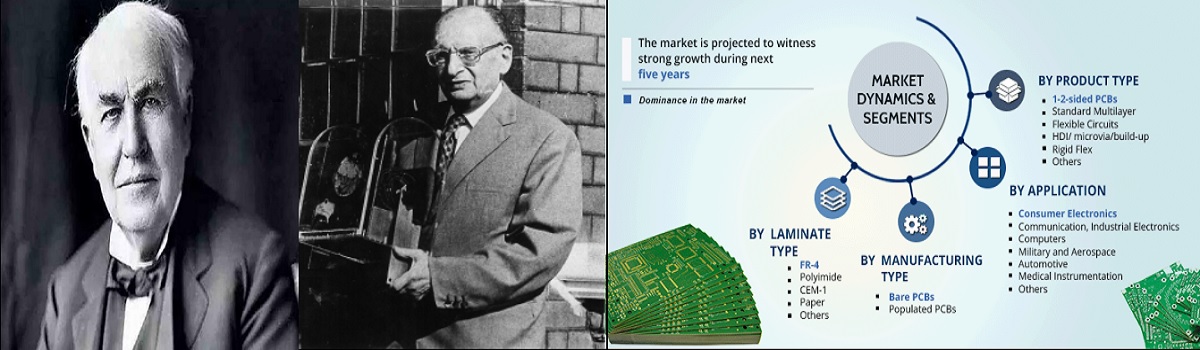
1). History: Albert Hanson invents first circuit board. Consisted of multiple layers. Filed for a patent in 1903. In 1904 Thomas Edison Plating conductor onto linen. Utilized through-hole connectivity. in the U.K. Paul Eisler invents the firstprinted circuit board. He developed a PCB for a radio system in 1936. The Institute for Printed Circuits (IPC) is formed in 1957. International Business Machines introduces planar mounting, which was developed in 1960. This technology today is known as SMT (Surface mount Technology). In 1980’s Gerber format was developed by Gerber scientific. Vapor Computerized Systems introduce CAM software and file format. Genesis 2000 software released in 1992. ODB++ data file format released to the public in 1997. Multek introduced Every Layer Interconnect (ELIC) for high density PCBs, was developed in 2006. Today, highly complex PCB can be designed and manufactured using CAD system. Also, CNC machines are used for fabrication. |
2). Printed Circuit Board Market: According to Govt Make in India and National policy on Electronics 2019, electronics manufacturing schemes like PLI, SPECS and EMC 2.0 have been launched. The Indian PCB market in India was worth US$ 2.78 Billion in 2019. Over the past few years, the demand for PCBs in India has witnessed a steady rise on account of increasing investment in digitization and favorable government initiatives. Looking forward, the PCB market in India is projected to reach US$ 6.33 Billion by 2024, exhibiting a CAGR of 17.9% during 2019-2024.PCBs are the back bone of the electronics industry as it is deployed in almost all the electronic products from consumer gadgets to industrial high-tech products.The Indian electronic devices market has witnessed double digit growth rates driven by rising disposable incomes and increasing urbanization levels in the country. Keeping PCB design as a skill will be highly helpful in core electronics manufacturing industry. |
|
|
|
|
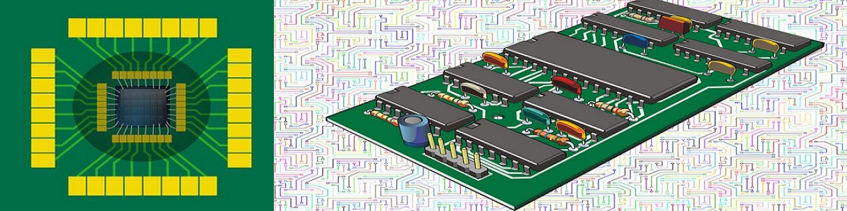
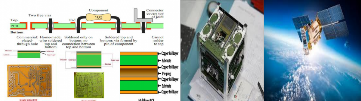
3). PCB and its types: A printed circuit board (PCB) mechanically supports and electrically connects electrical or electronic components using conductive tracks, pads and other features etched from one or more sheet layers of copper laminated onto and between sheet layers of a non-conductive substrate. Printed circuit boards are used in all but the simplest electronic products. They are also used in some electrical products, such as passive switch boxes. The PCB are divided into layers to decrease the complexity during design, so generally we describe these layers as top layer and bottom layer in PCB for DSB board. According to layers PCB is Classified as Single sided Board (SSB), Double sided Board(DSB), Multi-layer Board(MLB). According to material, Rigid and Flexible Board and metal PCB. |
4). Application area of PCB: From kitchen appliances to smartphones to microwaves, electronics play an essential role in our daily routines. Found at the heart of almost all electronics is a PCB or printed circuit board. In the modern world, PCBs act as the significant functional centers of almost all electronic devices. These small chips come in an uncountable number of several configurations and manufactured with different types of materials. Some of the application area includes: Medical devices, LEDs, Consumer Electronics, Industrial Equipment, Automotive Components, Aerospace Equipment’s, Maritime Application, Safety and Security devices, etc. the use of PCB is ever growing. In above applications designing a PCB plays crucial role. As it will cut down much of the cost of manufacturing. |
|
|
|
|
5).Tools for PCB Design: The designing of PCB can be done by manual drafting the PCB footprints and symbols using puppets, stickers or stencils. The common practice to design a PCB is by using Grid Paper(2.54mm). Later, we can draft a good layout and provide interconnection. In computer, we do the PCB design by using CAD tools or software like, Ki-CAD, OrCAD, Altium Designer, Eagle and man more. There after we do process like developing, Etching, plating, Drilling, solder masking and silk-screen. |
6). Online Courses offered by NIELIT:
(2-week): Rs 2000/-(Including GST )
|
|
7). References: https://www.imarcgroup.com/indian-pcb-market https://www.youspice.com/235/2/ BOOKS: Printed Circuit Boardsby R.S. Khandpur. |
8). Registration and Contact Person: Mr. D. Ramarao:-9096106882 Mr. Pawan G. Alhat:- 7588672311 Mr. Yogesh Shejwal:-9604986493 Sample reading material:- Introduction to PCB Overview of PCB Design Layout planning and design |