Digital Electronics Lab
|
1. Course Objectives: To present a problem oriented introductory knowledge of Digital circuits and its applications. To focus on the study of electronic circuits. |
|
|
2. Course Outcomes: Upon successful completion of the course/Lab the students will be able to |
|
|
CO1: Understand different Number systems, Codes, Logic Gates, Boolean laws & theorems. CO2: Simplify the Boolean functions to the minimum number of literals |
CO3: Design & implement different types of combinational logic circuits using Logic gates.. CO4: Design & implement different types of sequential logic circuits using Flip Flops |
|
3. Main Equipment’s Available |
|
|
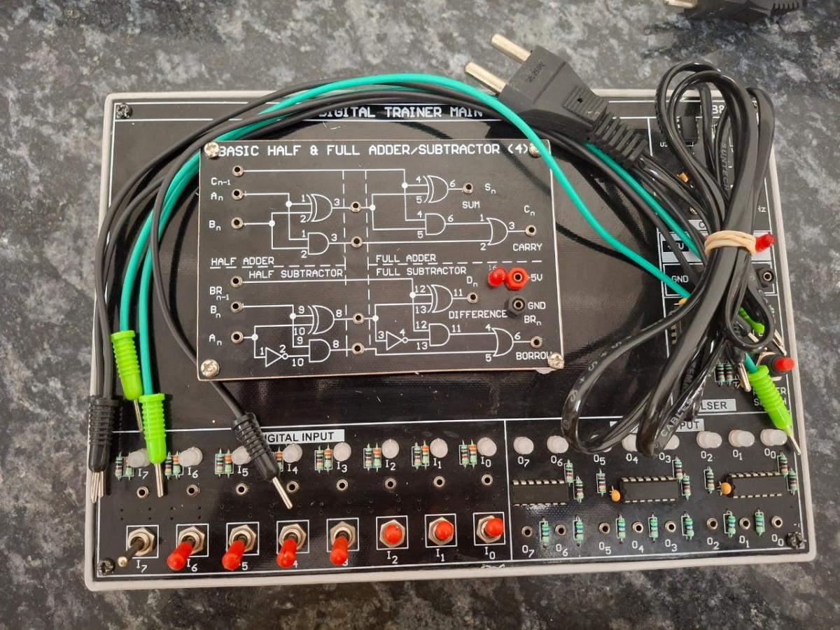
3.1 HALF AND FULLER ADDER/SUBTRACTOR: It is a arithmetic combinational logic circuit designed to perform addition/subtract of two single bits. It contain two inputs and produces two outputs. Outputs are called Sum and Carry/Borrow.
|
|
|
|
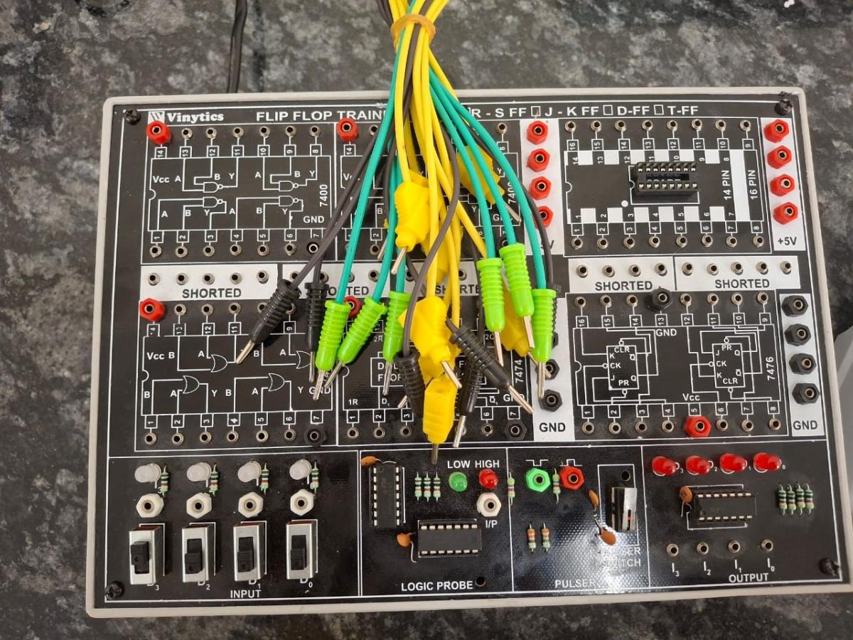
3.2 Flip-Flop Flip-Flop in digital electronics is a circuit with two stable states that can be used to store binary data. The stored data can be changed by applying varying inputs. Flip-flops and latches are fundamental building blocks of digital electronics systems used in computers, communications, and many other types of systems. Both are used as data storage elements. |
|
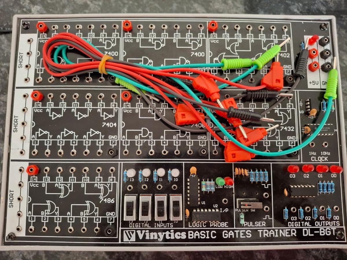
3.3 BASIC GATE TRAINER KIT A Logic gate is a kind of the basic building block of a digital circuit having two inputs and one output. The input and output relationship is based on a certain logic. These gates are implemented using electronic switches such as diodes, transistors. But, in practice, the basic logic gates are built using CMOS technology, MOSFET(Metal Oxide Semiconductor FET), FETS.
|
|
|
|
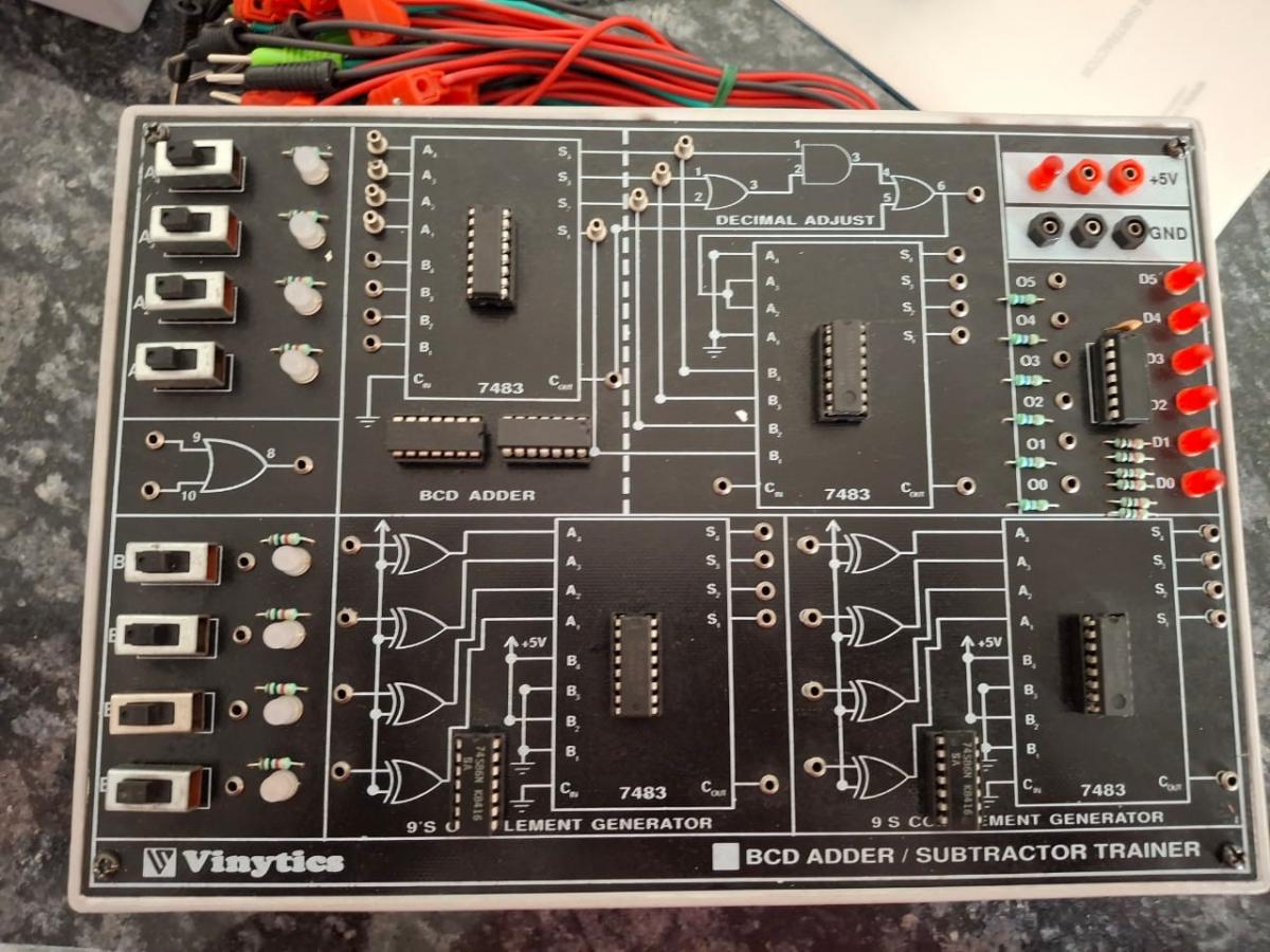
3.4 BCD BCD stands for binary coded decimal. It is used to perform the addition of BCD numbers. A BCD digit can have any of ten possible four-bit representations. Suppose, we have two 4-bit numbers A and B. The value of A and B can vary from 0(0000 in binary) to 9(1001 in binary) because we are considering decimal numbers |
|
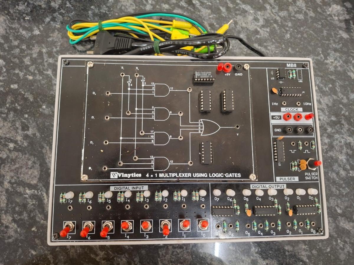
3.5 4x1 MULTIPLEXER USING LOGIC GATES A multiplexer is a combinational circuit that has 2n input lines and a single output line. Simply, the multiplexer is a multi-input and single-output combinational circuit. The binary information is received from the input lines and directed to the output line. Based on the values of the selection lines, one of these data inputs will be connected to the output. Unlike the encoder and decoder, there are n selection lines and 2n input lines. So, there is a total of 2N possible combinations of inputs. |
|
|
4. Suggestive List of Experiments |
|
|
1 1. Realization of Basic/ Exclusive Logic Gates using Universal Logic Gate. 2. Verification of operation of Full Adder and Full Subtractor. 3. Design & verification of 4-bit binary adder/subtractor using binary adder IC. 4. Realization of operation of full adder and full subtractor using IC 74151/74153 MUX. 5. Design & verification of full adder and full subtractor using an inverted output 3 to 8 line decoder.
|
6. Design and verification of operation of a BCD Adder using IC 7483. 7. Realization of 4 X 1 MUX using basic gates. 8. Verification of operation of BCD to Seven segment code conversion using IC 7447. 9. Verification of Truth Tables of SR & D Flip flops. 10. Verification of Truth Tables of Master Slave JK Flip-Flop. 11. Design of BCD ripple counter. 12. Design of Universal Shift Register. 13. Logic implementation using programmable Devices (ROM , PLA, FPGA) |
|
5. Suggested Books: |
6. References |
|
https://en.wikipedia.org/wiki/Digital_electronicshttps:// https://www.javatpoint.com/digital-electronics https://www.digitalelectronicsdeeds.com/ https://circuitverse.org/ https://test.sanfoundry.com/digital-circuits-tests/ https://www.tutorialspoint.com/digital_electronics/index.asp |
|
FACULTY COORDINATOR: Dr. L Shyam Sunder Singh LAB INCHARGE: Monika |
LAB CO-INCHARGE: Ankita Sharma PLACE: Room#108, Ground Floor, CSED@NIELIT |

